• +91 90818 90903
  • circuitelectronics2016@gmail.com
  • sales.circuitelectronics@gmail.com

Service

PCB Design Layout

Our PCB layout and PCB design services and capabilities includes

img
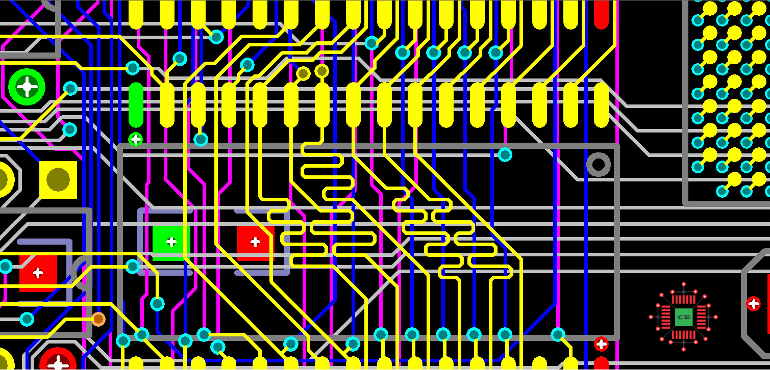
  • Single-sided, double-sided, and multi-layer boards (up to 16 layers) with high density design handing capabilities.
  • Component Library creation as per IPC standard.
  • Design for Surface mount, through-hole & mixed technology with QFN,BGA, PGA & fine pitch components.
  • Design as per EMI/EMC requirement.
  • Design for manufacturability (DFM)
  • Design for Assembly (DFA)
  • Bill of material generation.
  • Reverse Engineering (Bare board to design file/gerber)
  • Gerber Generation
  • Stack up creation for Multilayer.

PCB Reverse Engineering

We can take your sample, including components, and completely reverse engineer it. We create all the data you need to make duplicates. We can even reverse engineer boards that include programmed IC’s, custom parts, and obsolete parts. To begin, we identify every component on the board.

Gerber Validation

img
  • Gerber RS274D to RS274X file format conversion.
  • Design/Manufacturer rule checking (DRC/MRC)
  • Complete Gerber database validation for manufacturability.
  • PCB Penalization as per DFM/DFA requirement.
  • NC drill program generation & optimization.
  • Rout Master program generation.
  • BBT program generation as per Machine compatibility.
  • Glue & Paste Stencil design as per SMT requirement.

PCB Assembling (Though hole & SMT)

Everything from our smart phones to our cars includes electronic components. … A PCB with components mounted on is called an assembled PCB and the manufacturing process is called PCB assembly or PCBA for short. The copper lines on bare board, called traces, electrically link connectors and components to each other.